- 您现在的位置:买卖IC网 > Sheet目录1992 > CY28547LFXCT (Silicon Laboratories Inc)IC CLOCK CK505/410M INTEL 72QFN
CY28547
.......................Document #: 001-05103 Rev *B Page 2 of 24
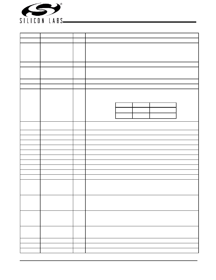
Pin Description
Pin No.
Name
Type
Description
1, 49, 54, 65 VDD_SRC
PWR
3.3V power supply for outputs.
2, 3, 52, 53,
55, 56, 58,
59, 60, 61,
63, 64, 66,
67, 69, 70
SRCT/C[2:9]
O, DIF 100-MHz Differential serial reference clocks.
4, 68
VSS_SRC
GND
Ground for outputs.
5, 6
CPUT2_ITP/SRCT10,
CPUC2_ITP/SRCC10
O, DIF Selectable differential CPU or SRC clock output.
ITP_SEL = 0 @ pin 39 assertion = SRC10
ITP_SEL = 1 @ pin 39 assertion = CPU2
7
VDDA
PWR
3.3V power supply for PLL.
8
VSSA
GND
Ground for PLL.
9
PGMODE
I, PU
3.3V LVTTL input for selecting the polarity of pin 39
Internal pull-up resistor of 100K to 3.3V, use 10K resistor to pull it low externally
if needed
10, 11
CPUC1_MCH,
CPUT1_MCH
O, DIF Differential CPU clock output to MCH
12
VDD_CPU
PWR
3.3V power supply for outputs.
13, 14
CPU[T/C]0
O, DIF Differential CPU clock output
15
VSS_CPU
GND
Ground for outputs.
16
SCLK
I
SMBus-compatible SCLOCK.
17
SDATA
I/O, OD SMBus-compatible SDATA.
18
VDD_REF
PWR
3.3V power supply for outputs.
19
XOUT
O, SE 14.318-MHz crystal output.
20
XIN
I
14.318-MHz crystal input.
21
VSS_REF
GND
Ground for outputs.
22
REF1
O
Fixed 14.318-MHz clock output.
23
REF0/FSC_TESTSEL
I/O
Fixed 14.318 clock output/3.3V-tolerant input for CPU frequency
selection/Selects test mode if pulled to VIMFS_C when pin 39 is asserted LOW.
Refer to DC Electrical Specifications table for VILFS_C,VIMFS_C,VIHFS_C specifi-
cations.
24
CPU_STP#
I
3.3V LVTTL input for CPU_STP# active LOW
During direct clock off to M1 mode transition, a serial load of BSEL data is driven
on this pin and sampled on the rising edge of PCI_STP#. See Figure 14.for more
information.
25
PCI_STP#
I
3.3V LVTTL input for PCI_STP# active LOW
During direct clock off to M1 mode transition, a serial load of BSEL data is driven
on CPU_STP# and sampled on the rising edge of this pin. See Figure 14. for more
information.
26, 28, 29,
38, 46, 57,
62, 71, 72
CLKREQ[1:9]#
I
3.3V LVTTL input for enabling assigned SRC clock (active LOW).
27
PCI1
O, SE 33MHz clock output
30, 36
VDD_PCI
PWR
3.3V power supply for outputs.
31, 35
VSS_PCI
GND
Ground for outputs.
PGMODE CLK mode Pin 39
0
CK410
VTT_PWRGD#/PD
1(default)
CK505
CK_PWRGD/PD#
发布紧急采购,3分钟左右您将得到回复。
相关PDF资料
CY28548ZXC
IC CLK CK505 960M/965M 64TSSOP
CY28551LFXC-3T
IC CLOCK INTEL/AMD SIS VIA 56QFN
CY28551LFXC
IC CLOCK INTEL/AMD SIS VIA 64QFN
CY2SSTV855ZXI
IC CLOCK DIFFDRV PLL DDR 28TSSOP
CY2SSTV857ZXI-27
IC CLK DDR266/333BUF1:10 48TSSOP
CY2SSTV857ZXI-32
IC CLK DDR266/333BUF1:10 48TSSOP
CY505YC64DT
IC CLK CK505 BROADWATER 64TSSOP
CYW150OXC
IC CLOCK 440BX AGP 56SSOP
相关代理商/技术参数
CY28548ZXC
功能描述:时钟发生器及支持产品 Intel 960/965M Crest line CK505 Intg Vreg RoHS:否 制造商:Silicon Labs 类型:Clock Generators 最大输入频率:14.318 MHz 最大输出频率:166 MHz 输出端数量:16 占空比 - 最大:55 % 工作电源电压:3.3 V 工作电源电流:1 mA 最大工作温度:+ 85 C 安装风格:SMD/SMT 封装 / 箱体:QFN-56
CY28548ZXCT
功能描述:时钟发生器及支持产品 Intel 960/965M Crest line CK505 Intg Vreg RoHS:否 制造商:Silicon Labs 类型:Clock Generators 最大输入频率:14.318 MHz 最大输出频率:166 MHz 输出端数量:16 占空比 - 最大:55 % 工作电源电压:3.3 V 工作电源电流:1 mA 最大工作温度:+ 85 C 安装风格:SMD/SMT 封装 / 箱体:QFN-56
CY28551
制造商:CYPRESS 制造商全称:Cypress Semiconductor 功能描述:Universal Clock Generator for Intel, VIA, and SIS㈢
CY28551-3
制造商:CYPRESS 制造商全称:Cypress Semiconductor 功能描述:Universal Clock Generator for Intel, VIA and SIS㈢
CY28551LFXC
功能描述:时钟发生器及支持产品 Universal System Clk Intel AMD SiS Via RoHS:否 制造商:Silicon Labs 类型:Clock Generators 最大输入频率:14.318 MHz 最大输出频率:166 MHz 输出端数量:16 占空比 - 最大:55 % 工作电源电压:3.3 V 工作电源电流:1 mA 最大工作温度:+ 85 C 安装风格:SMD/SMT 封装 / 箱体:QFN-56
CY28551LFXC-3
功能描述:时钟发生器及支持产品 Universal System Clk Intel AMD SiS Via RoHS:否 制造商:Silicon Labs 类型:Clock Generators 最大输入频率:14.318 MHz 最大输出频率:166 MHz 输出端数量:16 占空比 - 最大:55 % 工作电源电压:3.3 V 工作电源电流:1 mA 最大工作温度:+ 85 C 安装风格:SMD/SMT 封装 / 箱体:QFN-56
CY28551LFXC-3T
功能描述:时钟发生器及支持产品 Universal System Clk Intel AMD SiS Via RoHS:否 制造商:Silicon Labs 类型:Clock Generators 最大输入频率:14.318 MHz 最大输出频率:166 MHz 输出端数量:16 占空比 - 最大:55 % 工作电源电压:3.3 V 工作电源电流:1 mA 最大工作温度:+ 85 C 安装风格:SMD/SMT 封装 / 箱体:QFN-56
CY28551LFXCT
功能描述:时钟发生器及支持产品 Universal System Clk Intel AMD SiS Via RoHS:否 制造商:Silicon Labs 类型:Clock Generators 最大输入频率:14.318 MHz 最大输出频率:166 MHz 输出端数量:16 占空比 - 最大:55 % 工作电源电压:3.3 V 工作电源电流:1 mA 最大工作温度:+ 85 C 安装风格:SMD/SMT 封装 / 箱体:QFN-56